The Computer History Museum has two operational IBM 1401 computers used for demos, but a few weeks ago one computer suddenly couldn't print anything. I helped track down the problem, but it was more tricky than we expected; along the way we had to investigate the printer error checking circuits, the print buffer, and even low level core memory signals. This blog post discusses our investigation and how we traced the problem to a failed germanium transistor.
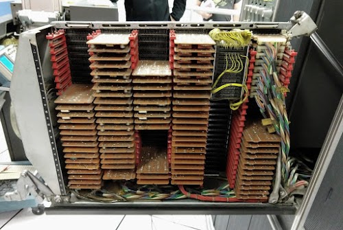
The IBM 1401 computer was announced in 1959, and went on to become the best-selling computer of the mid-1960s, with more than 10,000 systems in use. The 1401 leased for $2500 a month (about $20,000 in current dollars), a low price that let even medium-sized businesses use the 1401 for payroll, accounting, invoicing, and many other tasks. The IBM 1401 computer was constructed from small circuit boards (called SMS cards) plugged into units called "gates"—these are gates in the sense of something that swings open, not logic gates. The photo below shows the 1401 with one of the gates open, revealing dozens of brown SMS cards plugged into the gate.
One key selling point of the IBM 1401 was its high-speed line printer (the IBM 1403), which could hammer out 10 lines per second. (IBM claimed this was four times as fast as competing printers, but others dispute this.) The 1403 printer had excellent print quality, said to be the best printing until laser printers were introduced in the 1970s.1 IBM claims that "Even today, it remains the standard of quality for high-speed impact printing."
The 1403 printer used a chain of type slugs (above) that rotated at high speed above the paper, with an inked ribbon between the paper and the chain. Each of the 132 print columns had a hammer and an electromagnet. At the right moment, when the desired character passed the hammer, the electromagnet drove the hammer against the back of the paper, causing the paper and ribbon to hit the type slug, printing the character.2
Unfortunately, the printer at the Computer History Museum recently had a problem: whenever a line was printed, the computer would halt due to a "print check" error. Fortunately the museum has a team of volunteers to help keep the system running; people helping with this printer problem included Ron Williams, Frank King, Marc Verdiell, Carl Claunch, Michael Marineau, Robert Garner and Alexey Toptygin. By the time I arrived to help, Ron had written a simple test program that repeatedly attempted to print a line; he toggled the program into the computer by hand, and he disabled the error check. The printer printed the characters properly, so we suspected the problem was in the error reporting circuitry inside the computer. Our strategy was to find the error signal and then trace it back through the computer to determine why it was being generated.
We started by examining the latch circuit that holds the print check error condition and sends it to the rest of the computer. To find the circuit, we consulted the documentation: binders of cryptic computer-generated wiring diagrams, called Automated Logic Diagrams (ALD). A small piece of an ALD is shown below showing the print check latch (PR CHK LAT). Each box on the ALD corresponds to a circuit on an SMS board and the lines show how the boards are wired together. Deciphering the text inside the box on the right indicates a board of type 2JMX implementing a "2+AO" function, which in modern terms is AND-OR-Invert. The text in each box also indicates the location of the card: its gate (physical swing-out gate, not logic gate), gate 01A6 in this case, and the card's position in the gate (F10). Thus, to check the output (labeled H) of the latch with the oscilloscope, we swung out gate 01A6, found card F10, and hooked the oscilloscope to pin H. We found pin H went low (error) when pins F and G went high, which was the proper behavior for the latch. Pin G (PR CK SAMPLE) was essentially a clock to sample the error state, while pin F was the error signal itself. Our next task was to determine what was triggering the error signal on pin F.
The documentation also includes logic diagrams that show the circuitry at a logical level, which is slightly easier to understand than the physical connections on the ALD diagrams. The logic diagram below shows the printer error circuitry. At the right, the print check error signal (PRT CHK ERROR) comes out of the latch (PR CHK LAT) that holds the error signal. (This is the same latch as in the ALD diagram above, and you can match up the signal names.) To the left of the latch, several different error conditions are detected and combined to form the error signal fed into the latch. (Note that IBM's logic symbols didn't match standard symbols. The semicircle is an OR gate, not an AND gate. The triangle is an AND gate. An "I" in a box is an inverter.)
Several different conditions can trigger a print check error3 and we thought the "hammer fire" check was a likely candidate. Recall that the printer uses 132 hammers, one per column, to print a line of characters. To make sure the hammers are operating correctly, the computer has two special planes in core memory. (The 1401 contains 4,000 characters of core memory4; each bit of memory is a tiny ferrite ring that is magnetized one way to store a "1" and the other way for a "0". A grid of 4000 cores forms a plane, storing a 1-bit slice of memory. Multiple planes are stacked up to form the storage unit.) Each time the computer decides to fire a hammer, it records this in core memory in the "equal check" plane. When a hammer actually fires, the current pulse from the electromagnet stores a bit in the "hammer-fire" plane.5 Each print scan cycle, the computer compares the two core planes to see if a hammer was fired when it wasn't supposed to, or if a hammer failed to fire when it should have; a mismatch triggers the "hammer fire" check error.
After some difficulty6, we determined that the problem wasn't the hammer fire check, but a different check: "print line complete" (PLC). This check ensures that for each line, either exactly one character was printed in each column or the column was blank. This check uses a third special core plane, the "print line complete" plane. Each time a character is printed in a column, the corresponding bit is set. (For a blank or unprintable character, a separate circuit sets the column's bit.) At the end of the line (during scan 49), the print line complete cores are checked; if any core is zero, the printer failed to print that column and an error is reported. (You can see the PLC CHECK signal and the logic that generates it on the earlier logic diagram.)
Oscilloscope probing (below) showed that the PLC CHECK (yellow) was triggered because the system thought a second character was being printed in the same column. The cyan signal is the (inverted) PLC bit from core (PR LINE COMP LATCH); each low pulse indicates a character has been printed in that column. The pink pulse (PRINT COMPARE) indicates a new character is being printed. The problem is that the cyan and pink signals go low at the same time, indicating both an existing character and a new character in the column. This generates the extra blue pulse (PLC CHECK), which triggers the yellow pulse (PRINT CHK ERROR from the latch). (This circuit can be seen in the earlier logic diagram, labeled "Trying to print position twice".)
Several things could cause the system to think two characters were being printed in the column. Looking at the printer's output we saw that it printed just the expected character on the paper, so the circuit to print a character seemed to be working correctly (PRINT COMPARE, the single pink pulse above), We tested the blank / unprintable circuit and it was detecting blank and non-blank columns correctly. So the most likely problem was reading a 1 from core memory (the cyan line above, PR LINE COMP LATCH) when it should be a 0. But was the problem the wrong value going in to core, or the wrong value coming out?
The logic diagram below shows the circuit that writes to the Print Line Compare core memory. At the right, PR LINE COMP INH is the (inverted) signal written to core.8 On scan 49 (the error-checking print cycle after printing all 48 characters), this line is set high, clearing the memory. If a character is being printed, the PRINT COMPARE EQUAL signal will set the core. At the left, logic gates detect a blank or unprintable character. And if a 1 bit was already in core (PR LINE COMP LATCH), the 1 bit is rewritten to core.
We detected that this circuit was writing erroneous 1 bits to core because it was reading erroneous 1 bits from core. But that put us in a circle, not knowing if the initial problem was the read or the write. To resolve this, we triggered the oscilloscope on print scan 49, which is when the PLC bits get cleared, and then looked at the next print scan, which reads the cleared bits back. We saw 0's being written (i.e. PR LINE COMP INH high), but unexpectedly saw 1's coming back (PR LINE COMP LATCH). So we knew something was going wrong at a low level in the core memory.
I should mention that in the base 1401 system, the printer check bits were stored in the main core memory module, but our system used a separate "print storage" core memory for improved performance. The performance issue is due to how the printer uses core memory: each time a hammer lines up with a type slug, the computer reads the corresponding character from core memory and fires the hammer if the character in storage matches the character under the hammer. Since core memory is constantly in use while printing a line, the computer can't do any computation while printing. The solution was the print storage feature: an additional 132-address core memory that functioned as a print buffer.7 With print storage, a line to be printed was first rapidly copied from the main core memory to the print storage core memory. Then the computer could continue doing computation using the main core memory while the print circuitry read from the print storage core memory. Each option on the IBM 1401 had a monthly charge; IBM charged an extra $386 a month for the print storage feature.
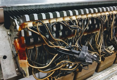
The photo above shows the gate that implements the print storage feature. The core memory module is the block on the upper right with yellow wires attached. (Individual cores can be seen in the photo below.) Core memory requires a lot of supporting circuitry. To select an address, driver cards generate X and Y signals. To write a core, the inhibit signal is combined with the clock by a gate, and then a driver card amplifies the signal and sends it through the inhibit line that passes through all the cores in the plane.8 When a core is read, it induces a pulse on a sense wire. This pulse is amplified by a sense amplifier card, and then the bit is stored in a latch. The numerous SMS cards in the print storage gate provided these support functions.
We probed the sense amplifier and latch cards on the reading side of the core memory and they seemed to be operating correctly, so we moved to the writing side. The HN inhibit driver card seemed a candidate for failure since it operates at high current, but we swapped the card with a replacement and the printer still failed. Next, I tried looking at the input to that card, but found there was no signal on that line, which seemed very suspicious.
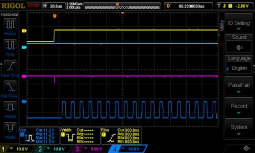
The missing signal was generated by a card of type CHWW, a NAND gate that combines the inhibit signal with the clock before sending it to the driver card. I hooked up the oscilloscope to the inputs and output of the NAND gate, yielding the trace above. This trace was the smoking gun: the output (cyan 2) remained high even when the two inputs (pink 3 and blue 4) went high. This showed that the NAND gate had failed and its output was stuck high. This explained everything: with this output stuck high, only 1's would be written to the PLC core plane. Then, when a character was printed, the print circuitry would read the 1 from core, think a character had already been printed in this column, the PLC check would fail, and the print check error would be triggered.
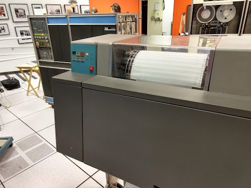
We swapped this card with a spare, and the printer started printing without any errors (above). This proved that we had finally traced the problem; it was a simple NAND gate in the depths of the printer buffer core memory circuit. The failed card is shown below. It implements three NAND gates (details) using diode-transistor logic (which IBM calls CDTL—Complemented Transistor Diode Logic). Each two-input gate uses one germanium transistor (circular metal can) and two diodes (striped glass components on the right). Pull up resistors (striped) and inductors (beige) on the left complete the circuits.
I tested the card with a signal generator and found that while two of the three NAND gates worked, the other was stuck at a high output, confirming what we saw inside the 1401. Next I tested the transistors using the diode test mode on a multimeter. The good transistors had voltage drops of 0.23V. (This may seem low, but remember that these are germanium transistors not silicon transistors.) In comparison, the bad transistor had a Vbe drop of 0.95V, much higher. Finally, we removed the transistors and checked them on a vintage Tektronix 577 curve tracer. We thought the bad transistor might just be too weak to operate the gate, but it was entirely dead—totally flatlined on the curve tracer.
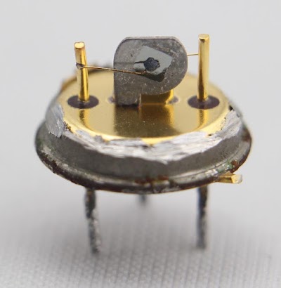
We opened up the transistor on a lathe and looked inside. The transistor is an IBM 083 NPN germanium alloy transistor (germanium was used before silicon transistors). The transistor consists of a tiny germanium die (the shiny metallic square below), forming the base. Two wires are attached for the emitter and collector, connected to dots of tin alloy, a larger dot on the front for the collector and a smaller dot on the back for the emitter. Under the microscope, it looked like there was some corrosion on the alloy dots and the emitter wire didn't look solidly connected, so we suspect that is the root cause of the failure.
Conclusions
This was a harder problem to diagnose than most of the IBM 1401 issues. But we managed to track down the problem, replace the bad card, and get the printer back in operation. One nice thing about the IBM 1401 compared to modern systems is that it's not a black box—you can look inside all the circuitry, down to the individual transistors. In this case, we were able to find the bad transistor that was causing the system failure, and even determine that it was probably corrosion that killed the transistor.
I announce my latest blog posts on Twitter, so follow me at @kenshirriff for future articles. I also have an RSS feed. The Computer History Museum in Mountain View runs demonstrations of the IBM 1401 on Wednesdays and Saturdays so if you're in the area you should definitely check it out (schedule).
Notes and references
-
One reason for the IBM 1403's high quality printing was its use of a type chain instead of typebars or a drum. Many earlier line printers used rows of typebars or a rotating drum of characters. Any timing imprecision would change the vertical positioning of characters, yielding ugly wavy text. The 1403, on the other hand, used a horizontally rotating chain of characters so misalignment caused a hardly-noticeable change in the spacing between characters. ↩
-
You might expect that the 132 hammers align with 132 type slugs, so the matching hammers all fire at once, but that's not what happens. Instead, the hammers and type slugs are spaced slightly differently, so only one hammer is aligned at a time, and a tiny movement of the chain lines up a different hammer and type slug. (Essentially they form a vernier.) Specifically, every 11.1 microseconds, the chain moves 0.001 inches. This causes a new hammer / type slug alignment. For mechanical reasons, every third hammer lines up in sequence (1, 4, 7, ...) until the end of the line is reached; this is called a "subscan" and takes 555 microseconds. Two more subscans give each hammer in the line an option to fire, forming a print scan of 1.665 milliseconds. 48 print scans give each hammer a chance to print each character, and then the 49th print scan is used for error checking. (For more details of this timing, see Manual of Instruction, page 37.)
The mechanism of scans and subscans may seem excessively complicated. But what it accomplishes is matching up the fast "electronic world" with the slower "mechanical world." Specifically, every 11.1 microseconds, a hammer and type slug line up. The computer reads the character in that column from core, compares it to the character on the type slug, and if they match, it fires the hammer. The important thing here is that a core memory cycle matches the time between hammer alignments, making it possible to read the character from core for each hammer alignment. If you want more information on how the print chain works, I have an animation here.
One subtlety is that a hammer takes 1.52 milliseconds to impact (Manual of Instruction, p32). Thus, it's not really the case that the hammer fires when it lines up with the type, but when it will be lined up 1.52 milliseconds in the future. ↩
-
It may seem excessive that the 1401 had multiple checks to ensure that the printer was operating properly. But for a business computer, print errors could be catastrophic: imagine if a day's payroll checks had a digit printed wrong or tax forms were printed incorrectly. IBM's scientific computers had much less error checking than the business computers, on the assumption that scientists would notice problems. ↩
-
The 1401 stores 4,000 characters in core memory, not 4096, because it is a decimal machine (i.e. BCD), with decimal addresses. Its memory can be expanded to 16,000 characters with a dishwasher-sized memory expansion unit; I wrote about repairing this unit here. I wrote more about the 1401's core memory here. ↩
-
Recording each hammer fire in core memory isn't done by the computer writing to core memory. Instead, each hammer is physically wired directly to a particular core; 132 wires from the hammer electromagnets to the cores. When a hammer fires, the current pulse from the hammer's electromagnet goes through a wire wrapped through the corresponding core, magnetizing that core. (You can see these wires in the earlier picture of the cores.) ↩
-
It was tricky to determine which signal was triggering the error input F, due to the 1401's use of wired-OR. Because transistors were expensive when the IBM 1401 was built, IBM used many tricks to reduce the transistor count. One trick is the wired-OR—instead of using an OR gate, signals are simply wired together so if any signal is high it will pull the line high. Thus, We couldn't simply probe the signals feeding into pin F because they were all wired together. Instead, we needed to disconnect cards so we could test one signal at a time. ↩
-
The print storage core memory has 12 core planes; that is, it stores 12 bits at each location. Like a regular core location, it uses 6 bits to store each BCDIC character, as well as a bit for the word mark (metadata indicating field locations), and a parity bit. In addition, the print storage has four planes for error detection: a hammer fire sense plane (recording the hammers that fired), equal check plane (recording the hammers that should fire), print line complete plane (recording columns with a character printed), and an error check plane (indicating the column that triggered an error). ↩
-
The process to write to core memory may seem backwards, using a high signal on the inhibit line to write a 0. This is due to how cores function. The key that makes cores work is that they require a high current pulse to flip the core's magnetic state; a pulse with half the current has no effect on the core. Cores are arranged in a grid, with X and Y address lines that are pulsed to select a core. Multiple planes are stacked, one for each bit. Each line is pulsed with half the necessary current, so only the core where both lines cross has enough current to flip to the 1 state. Each plane has an inhibit line that passes through all the cores in the plane. To write a 1 to a plane, the inhibit line gets no current, causing the addressed core to flip to 1 as described. To write a 0 to a plane, the inhibit line gets half current in the opposite direction. The result is that none of the cores get enough current to flip, and the addressed core remains in the 0 state. Thus, by setting each plane's inhibit line appropriately, the desired 0's and 1's can be written to the address in the core stack. ↩
-
For information on how the print checks work, see Instruction Logic, page 98. The 1403 printer is documented in IBM 1403 Printer Component Description, 1403 Printers Field Engineering Maintenance Manual and 1403 Printers Field Engineering Manual of Instruction. See also this brief article about the 1403 printer in the IEEE Spectrum. For a detailed description of the IBM 1401, see IBM 1401: a modern theory of operation. ↩






7 comments:
It is so amazing to see how stuff was done at the beginning of electronic computation -- each bit, each gate was precious! (and it could be poked with your finger) I keep that in mind when I launch yet another scientific computation on 12000 cores. You are doing great work!
This was a very enjoyable article to read, better than some mystery novels!
You used a nice modern storage scope. How much harder would this be with an analog scope? Is that what field service used?
Regarding note 2 and the page with animation: The mechanism of scans and subscans not only matches electronic world to mechanical world, but also prevents things like someone like me trying to print a magic line of text the would fire every hammer at the same time, which would surely draw too much current or put too much drag on the system, and blow it up. Instead it spreads out the electrical and mechanical load, and thwarts such attempts. Brilliant!
I'm convinced all of these ideas will be needed again when we move to nanotech.
Dithermaster: back in the 1960s, field service had analog scopes. It was easier with a modern scope (in particular, 4 channels made it much easier to figure out what was going on), but I'm sure they did fine with analog scopes.
LOL, i came here with the same idea, how did they do it without that nice digital stuff :)
https://www.oscilloscopemuseum.com/collection-tek.html lots of scopes but don't see any multi channel so a bit more work to find the problem
Wow! A blast from the past. I learned computer maintenance using a Xerox Sigma 2 computer back in the 1970s. The computer was used in a Westinghouse Prodac-250 at a power station. I remember spending hours and hours wading through logic diagrams in large books to troubleshoot the computer. This sure brought back some of those (now fondly remembered) memories.
Have you tried turning it off and on? ;)
I was the systems programmer for a real mainframe the 7040 scientific computer back in 1965. It used a 1401 as it's card/reader/punch and printer. A little bit of commercial accounting was also run on the 1401. The 1410 which was a machine somewhat similar to the 1401 was more of a commercial main frame.
Post a Comment